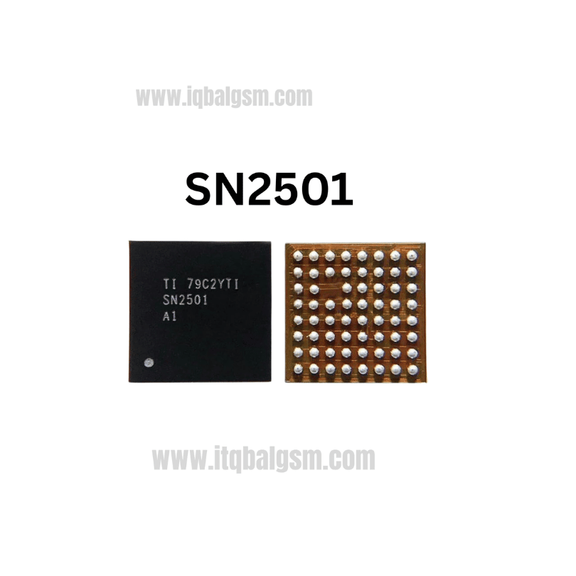
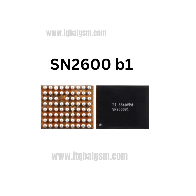
98611 IC
As low as
Rs 260.00
Worldwide shipping · Cash on Delivery
Product Details
--------------------------------------------------------------------------------
SECTION 1: INTERNAL ARCHITECTURE & CIRCUIT SCHEMATIC ROLES
--------------------------------------------------------------------------------
1. Dual Rail Display Power Supply Generation (Bias Rails):
- AVDD (+5.0V to +5.5V DC): Generated via an internal synchronous step-up converter and clean low-dropout (LDO) regulator to power source driver circuits of the TFT/LCD screen.
- AVEE (-5.0V to -5.5V DC): Generated via an on-chip inverting charge pump, providing clean negative rail reference for liquid crystal switching.
2. 3-Channel LED Backlight Driver:
- Boost Switching Pin (LX / LXBST): Drives an external SMD power inductor (typically 4.7µH to 10µH) to boost battery voltage (3.8V) up to 18V–25V DC depending on the series LED string count.
- Integrated Current Sinks (CH1, CH2, CH3): Provide precision current matching (±2.2% at 1mA) to eliminate color shifting and ensure perfectly uniform brightness across the entire LCD backlight grid.
--------------------------------------------------------------------------------
SECTION 2: BOARD-LEVEL TROUBLESHOOTING & COMMON FAULT SYMPTOMS
--------------------------------------------------------------------------------
1. Dark Screen with Normal Phone Operation (No Backlight):
- Phone boots completely, incoming ringers sound, and touch feedback vibrates, but the display backlight remains 100% dark.
- Root Cause: Failed boost switching FET inside the ISL98611, open-circuit boost inductor, blown Schottky boost diode, or fractured solder balls beneath the chip.
2. Blank White or Totally Black Display (No Image, No Light):
- Neither the backlight nor the image graphics appear.
- Root Cause: Loss of the ±5V bias rails (AVDD / AVEE) due to internal charge pump failure in the ISL98611, leaving the display driver unpowered.
3. Logic Board VBAT Dead Short:
- Connecting the logic board to a DC power supply immediately causes current to peg at 2A–5A with 0V displayed.
- Root Cause: Internal punch-through breakdown across the high-side input MOSFET connecting the VBAT power bump directly to ground.
--------------------------------------------------------------------------------
SECTION 3: STEP-BY-STEP MULTIMETER DIAGNOSTICS & TEST POINTS
--------------------------------------------------------------------------------
1. Cold Testing (Diode Mode Drop Readings in mV):
- Set Multimeter to Diode Mode; place RED probe on Ground (PCB shielding frame), probe points with BLACK probe:
* VBAT / VIN Line Capacitor: Normal reading is ~350 mV to 450 mV. (0.000V indicates an active dead short).
* Backlight Boost Anode Line (VLED+): Normal diode drop across output filtering capacitor is ~500 mV to 650 mV.
* Backlight Cathode Return Lines (CH1/CH2/CH3): Each should read balanced (~600 mV to 750 mV).
* AVDD Output (+5V test pad): Healthy diode drop of ~450 mV to 550 mV.
* AVEE Output (-5V test pad): Healthy diode drop of ~500 mV to 600 mV.
2. Hot Testing (Phone Powered On with Display Connected):
- Measure DC Voltages with BLACK probe grounded:
* Boost Anode (VLED+): Must register between 18V and 24V DC when the screen turns on. If it stays at battery voltage (~3.8V), the 98611 boost converter is not oscillating.
* AVDD Line: Must measure steady +5.0V to +5.5V DC.
* AVEE Line: Must measure steady -5.0V to -5.5V DC.
--------------------------------------------------------------------------------
SECTION 4: SOLDERING, REBALLING & REWORK SPECIFICATIONS
--------------------------------------------------------------------------------
1. Safe Removal:
- Shield nearby plastic FPC connectors (LCD connector, battery connector) and sensitive memory ICs with aluminum foil tape and multiple Kapton tape layers.
- Apply a small bead of quality rosin flux (e.g., Amtech NC-559-V2-TF or Relife RL-422) around the 98611 perimeter.
- Hot Air Rework Station Settings: 320°C - 330°C with 20% to 25% gentle airflow using a fine circular nozzle.
- Heat the 30-pin package evenly in small circles for 10–12 seconds until solder liquefies. Carefully lift the chip vertically using fine micro-tweezers.
2. Motherboard Footprint Cleanup:
- Add a tiny amount of 183°C leaded solder to the pads to reduce alloy melting point.
- Clean the 30 micro-pads gently using 0.6mm desoldering braid at 300°C–310°C without applying downward force to avoid tearing fragile solder pads.
- Scrub the footprint thoroughly with 99.9% pure Isopropyl Alcohol (IPA) and inspect under microscope for pad flatness and absence of bridging.
3. Reballing & Installation of New ISL98611 (98611):
- Use a dedicated 30-pin / universal 0.35mm–0.4mm pitch WLCSP stencil.
- Spread 183°C medium-temperature solder paste smoothly; heat with hot air at 250°C–260°C until perfect, uniform spherical balls form.
- Coat the motherboard footprint with a micro-thin, transparent layer of tacky flux.
- Orient Pin 1 index dot precisely according to the board silkscreen guide.
- Solder at 320°C with 20% airflow. Watch for the chip to float and settle automatically onto its pads via surface tension. Give a gentle microscopic nudge to ensure proper seating.
- Allow PCB to cool naturally for 2 minutes, clean flux residue with IPA, reassemble the display assembly, and verify bright, clear backlight and crisp graphics.
You may also like