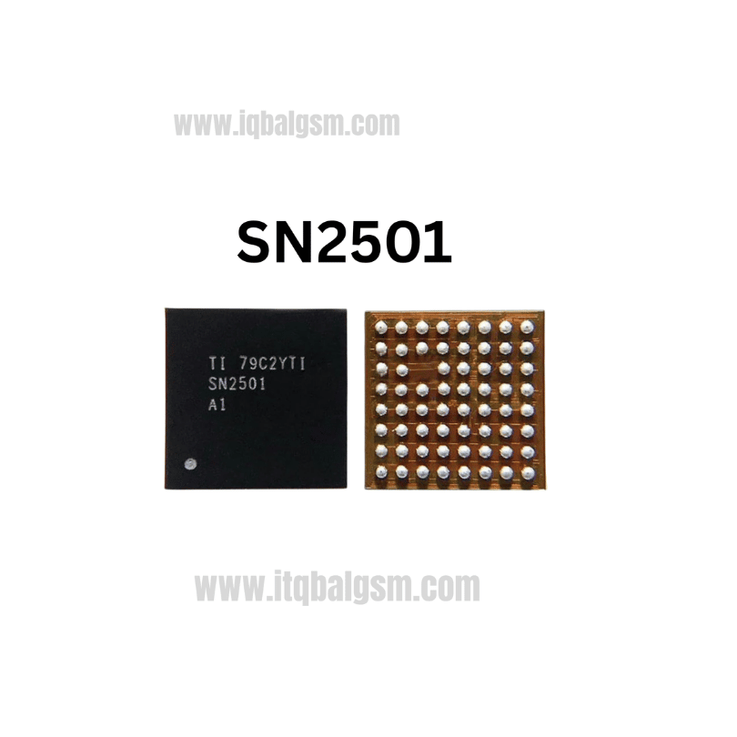
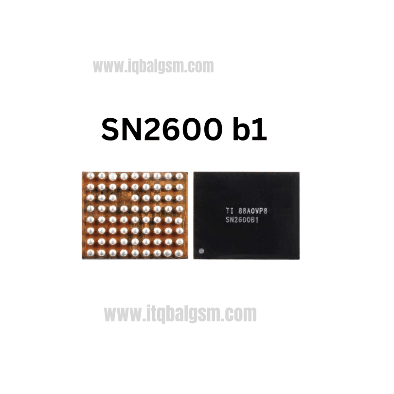
98512 IC
As low as
Rs 280.00
Worldwide shipping · Cash on Delivery
Product Details
--------------------------------------------------------------------------------
SECTION 1: INTERNAL ARCHITECTURE & CIRCUIT TOPOLOGY
--------------------------------------------------------------------------------
1. Digital Audio & Control Bus Interfacing:
- Digital Audio Input (I2S / PCM / TDM / SoundWire): Receives digital PCM audio data streams directly from the Qualcomm / Exynos audio subsystem codec.
- I2C Control Bus (SDA / SCL): Communicates dynamic volume levels, power-state transitions, mute commands, thermal status, and diagnostic flags to the host Application Processor.
- Closed-Loop Transducer Protection: On-chip voltage and current monitoring ADCs continuously track speaker voice-coil temperature and mechanical excursion to prevent blowout.
2. Boost Converter & Class-D Output Stage:
- Integrated Synchronous Step-Up DC-DC Converter: Boosts battery voltage (3.6V–4.2V) up to ~8V–10V dynamically during high-amplitude audio passages.
- Class-D Filterless Bridge-Tied Load (BTL) Drivers (SPK_OUT+ / SPK_OUT-): Feeds differential audio drive power to the bottom ringer and/or stereo earpiece speaker contacts through ferrite beads and EMI suppression filters.
--------------------------------------------------------------------------------
SECTION 2: BOARD-LEVEL TROUBLESHOOTING & COMMON FAULT PATTERNS
--------------------------------------------------------------------------------
1. Complete Speaker / Ringer Silence:
- Smartphone displays normal audio playback progress bar on screen, but zero sound comes from the loudspeaker.
- Root Cause: Missing VBAT power supply, blown external boost inductor, cracked solder bumps underneath the MAX98512, or an open-circuit series ferrite bead on the speaker lines.
2. Audio Distortion / Rattling / Crackling at High Volume:
- Sound is relatively clean at low levels, but clips severely, rattles, or cuts off completely as the volume slider is pushed past 60%.
- Root Cause: Degradation of the internal boost switching FETs, causing the internal boosted supply rail to collapse under heavy acoustic load.
3. System Lockup / Reboot on Ringtone Trigger:
- The device freezes, crashes to black, or reboots whenever an incoming call or alarm triggers.
- Root Cause: Broken solder joints under the I2C bus pins pulling the processor's communication lines low and triggering a kernel watchdog reset.
4. Direct VBAT / VPH_PWR Short Circuit:
- Connecting the board to a DC power supply instantly draws 2A–5A at 0V with immediate heating around the audio IC area.
- Root Cause: Internal punch-through breakdown inside the high-side power MOSFET connecting VBAT bumps directly to GND.
--------------------------------------------------------------------------------
SECTION 3: MULTIMETER DIAGNOSTICS & TEST POINTS
--------------------------------------------------------------------------------
1. Cold Testing (Diode Mode Drop Readings in mV):
- Set Multimeter to Diode Mode; place RED probe on Logic Board Ground (metal shield frame), probe surrounding test components with BLACK probe:
* VBAT Power Input Line: Healthy reading is ~350 mV to 450 mV. (0.000V indicates an active dead short).
* Boost Inductor Terminals: Should read ~350 mV to 450 mV on both pins with near-zero milliohms across the coil.
* Speaker Output Lines (SPK_OUT+ / SPK_OUT-): Must show closely matched diode drops (~550 mV to 650 mV, difference <15 mV).
* I2C Bus Pins (SDA / SCL): Normal reading is ~450 mV to 550 mV with pull-up behavior.
2. Hot Testing (Phone Powered On & Audio File / Ringtone Playing):
- Measure DC Voltages with BLACK probe grounded:
* VBAT Line: Steady 3.8V to 4.2V DC.
* Boost Output Filter Capacitor: During loud playback, voltage should dynamically step up from battery voltage to ~7.5V–9.5V DC. If it remains frozen at 3.8V, the boost circuit inside the MAX98512 is dead.
* Speaker Lines: Stable DC bias with active AC millivolts responding to music rhythm.
--------------------------------------------------------------------------------
SECTION 4: SOLDERING, REBALLING & REWORK SPECIFICATIONS
--------------------------------------------------------------------------------
1. Safe Removal Procedure:
- Shield neighboring heat-sensitive components (CPU, UFS storage, camera sockets, and battery connector) with multi-layer Kapton tape and thick aluminum heatsink foil.
- Dispense a moderate bead of high-grade tacky rosin flux (e.g., Amtech NC-559-V2-TF or Relife RL-422) around the chip boundary.
- Hot Air Station Settings: 330°C - 340°C with 20% to 25% airflow using a fine circular nozzle.
- Heat in a smooth, continuous circular motion for 10–14 seconds. Once the micro solder balls melt, gently lift the chip vertically with fine micro-tweezers.
2. Motherboard Footprint Dressing:
- Add a tiny drop of 183°C leaded solder (Sn63/Pb37) across the footprint to lower the alloy melting temperature.
- Clean the pads gently using 0.6mm desoldering braid at 310°C without applying downward force to avoid tearing microscopic PCB pads.
- Clean thoroughly with 99.9% pure Isopropyl Alcohol (IPA) and inspect under microscope for pad flatness and absence of bridging.
3. Reballing & Installation of New MAX98512 (+98512):
- Use a dedicated WLCSP / universal 0.35mm–0.4mm pitch BGA stencil.
- Spread 183°C medium-temperature solder paste smoothly; heat with hot air at 250°C–260°C until perfect, uniform spherical balls form.
- Apply a micro-thin, transparent layer of tacky flux to the motherboard footprint.
- Carefully align Pin 1 corner index dot with the motherboard silkscreen white dot.
- Solder at 320°C with 20% airflow; the surface tension of the molten solder will automatically pull the chip into exact center alignment. Confirm with a microscopic tweezer touch.
- Allow PCB to cool naturally for 2 minutes, clean flux residue with IPA, reassemble the phone, and verify crystal-clear, loud stereo audio output.
You may also like