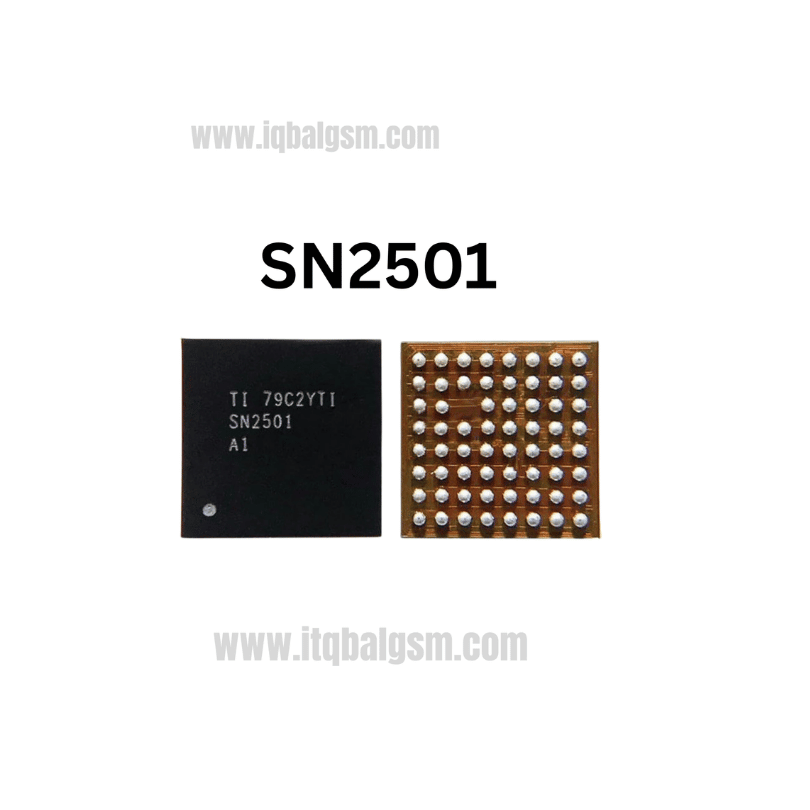
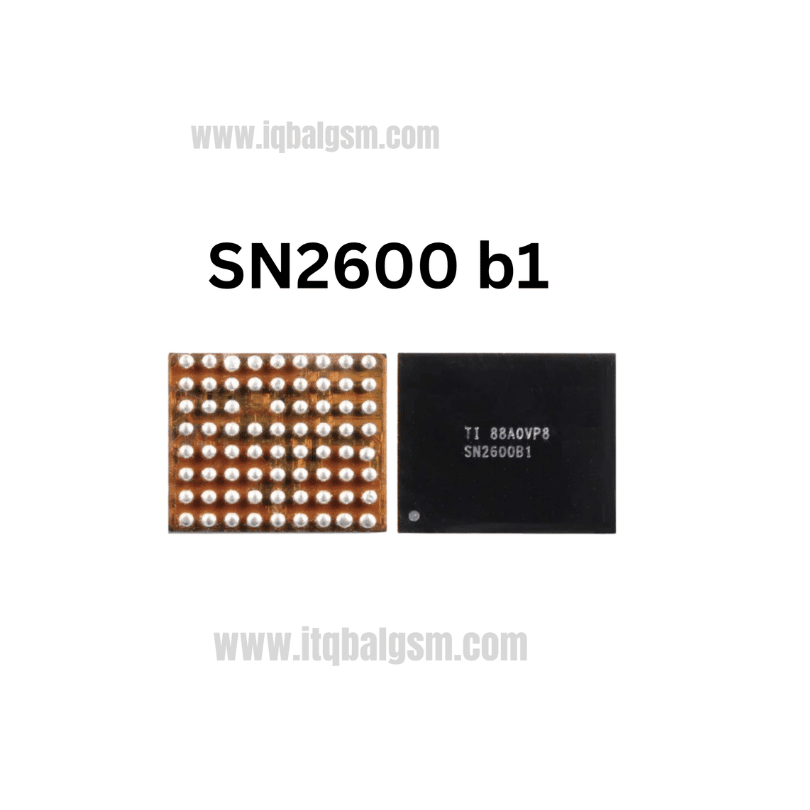
955 IC
As low as
Rs 280.00
Worldwide shipping · Cash on Delivery
Product Details
--------------------------------------------------------------------------------
SECTION 1: ELECTRICAL ARCHITECTURE & SIGNAL TOPOLOGY
--------------------------------------------------------------------------------
1. RX / TX Signal Routing:
- RX Down-Conversion Stage: Receives amplified RF signals from multi-band Low Noise Amplifiers (LNAs); down-converts RF carriers to differential baseband I/Q channels and routes them directly to the Exynos 8895 baseband modem.
- TX Direct Modulation Stage: Accepts baseband I/Q data streams from the modem, up-converts them to targeted cellular frequencies, and feeds the modulated RF drive signals into external Power Amplifiers (PA / FEM modules).
- Control Interface (RFFE / MIPI Bus): Synchronized by the baseband processor to control band switching, gain states, and carrier aggregation configurations in real time.
2. Power Distribution Network (PDN):
- Multiple LDO regulated rails supplied by the RF power management unit:
* 1.8V IO / Digital Core Supply (VDD_1P8)
* 1.2V / 1.0V Analog Transceiver Core Rails (VDD_1P0_RF / VDD_1P2_RF)
* Dedicated RF reference clock lines (26MHz / 38.4MHz TCXO)
--------------------------------------------------------------------------------
SECTION 2: BOARD-LEVEL TROUBLESHOOTING & COMMON FAULT PATTERNS
--------------------------------------------------------------------------------
1. "No Service" / Continuous Searching:
- Phone detects SIM card IMSI, but signal bars remain completely empty with "No Service" status.
- Manual search in Settings displays "Error while searching for networks".
- Cause: Defective Shannon 955 silicon, broken internal LNA switching matrix, or cracked BGA solder balls under U202 following a drop.
2. Unknown Baseband & Missing IMEI:
- Dialing *#06# displays a blank screen or missing IMEI; Settings > About Phone displays "Baseband Version: Unknown".
- Cause: Missing 1.8V VDD rail to U202 or fractured master clock/reset line preventing modem-to-transceiver handshake.
3. 1.8V Line Short Circuit (Phone Dead or Overheating):
- Power supply draws immediate short-circuit current (~1.2A to 2.0A) when prompt-booted.
- Multimeter measures direct short across decoupling capacitor C417 on the U202 1.8V supply rail (reads ~40Ω to 0.000V instead of normal >2.5 kΩ).
- Cause: Internal gate punch-through breakdown inside the Shannon 955 IC.
--------------------------------------------------------------------------------
SECTION 3: STEP-BY-STEP MULTIMETER TESTING & DIAGNOSTICS
--------------------------------------------------------------------------------
1. Cold Testing (Diode Mode Drop Readings in mV):
- Set Multimeter to Diode Mode; place RED probe on Ground (metal shielding can rim), probe peripheral components with BLACK probe:
* 1.8V Supply Rail Capacitor (C417 / C202 series): Normal reading is ~380 mV to 480 mV (Resistance mode must show >2.5 kΩ). A reading of 0.000V or under 50Ω proves an internal short.
* 1.0V / 1.2V Analog Supply Capacitors: Normal diode drop ~320 mV to 420 mV.
* RFFE Clock & Data Lines (CLK / DATA): Normal readings ~450 mV to 550 mV.
* TCXO Clock Input Pin: Normal diode drop ~500 mV to 620 mV.
2. Hot Testing (Phone Powered On with SIM Card Inserted):
- Measure DC Voltages with BLACK probe on Ground:
* VDD_1P8: Steady +1.8V DC.
* VDD_1P2 / VDD_1P0: Steady +1.2V and +1.0V DC respectively. If any supply rail collapses to 0V upon boot, inspect the RF-PMIC before lifting U202.
--------------------------------------------------------------------------------
SECTION 4: SOLDERING, REBALLING & REWORK SPECIFICATIONS
--------------------------------------------------------------------------------
1. Safe Removal:
- Carefully de-solder the RF metal shielding can using hot air at 340°C with shielding foil protecting the nearby Exynos CPU and UFS memory.
- Apply a small drop of quality rosin flux (e.g., Amtech NC-559 or Relife RL-422) around the U202 perimeter.
- Hot Air Settings: 330°C - 340°C with 25% airflow using a medium circular nozzle.
- Heat in a smooth, continuous circular motion for 12–15 seconds until the BGA solder balls liquefy; gently lift the IC vertically using fine tweezers.
2. Logic Board Pad Dressing:
- Apply a small amount of 183°C leaded solder (Sn63/Pb37) across the footprint to lower the melting temperature.
- Gently sweep 0.8mm desoldering braid at 310°C without applying downward force to avoid peeling microscopic RF signal pads.
- Clean the area thoroughly with 99.9% pure Isopropyl Alcohol (IPA) and inspect under microscope for pad flatness and absence of bridging.
3. Reballing & Installation of New Shannon 955:
- Use a dedicated Samsung Exynos 8895 / Shannon 955 BGA stencil (0.12mm thickness).
- Spread 183°C solder paste smoothly across all apertures; heat with hot air at 260°C until uniform spherical balls form.
- Apply a micro-thin, transparent coat of tacky flux on the cleaned motherboard pads.
- Align Pin 1 index dot precisely with the motherboard silkscreen white dot.
- Solder at 320°C with 20% airflow; the surface tension will automatically center the chip onto its pads. Confirm with a gentle microscopic nudge.
- Allow PCB to cool naturally for 2 minutes, clean flux residue with IPA, assemble the motherboard with antennas connected, insert a active SIM card, and verify instantaneous 4G/LTE signal reception and clear outgoing calls.
You may also like