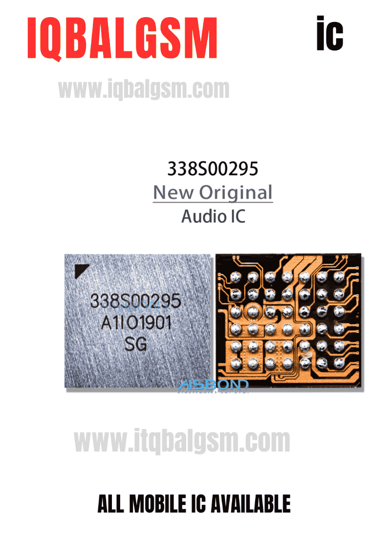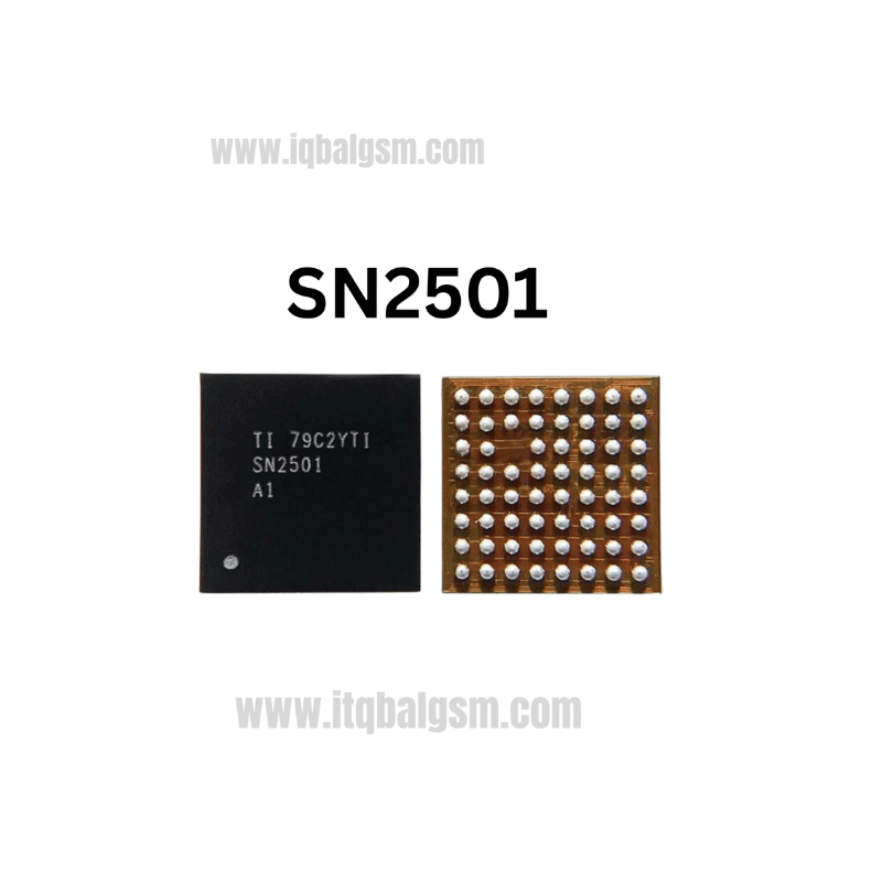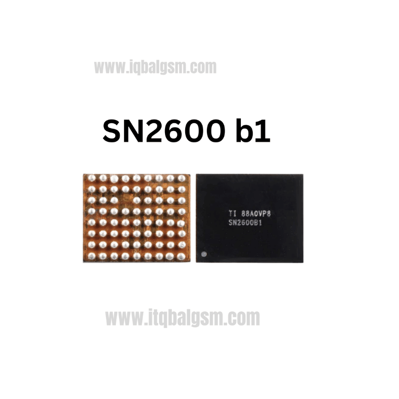

874B IC
As low as
Rs 250.00
Worldwide shipping · Cash on Delivery
Product Details
--------------------------------------------------------------------------------
SECTION 1: INTERNAL ARCHITECTURE & CIRCUIT OPERATION
--------------------------------------------------------------------------------
1. Digital Audio Bus & Control Interface:
- Digital Audio Stream (I2S / PDM / SoundWire): Receives digitized high-resolution audio samples directly from the SoC audio subsystem.
- I2C Command Lines (SDA / SCL): Dynamically controls hardware volume attenuation, EQ curves, sample rate switching, and internal diagnostics.
- Embedded Sensor Feedback: Monitors instantaneous voice-coil temperature and mechanical cone displacement through integrated high-speed voltage/current sensing loops.
2. Adaptive Boost Converter & Class-D Output Stage:
- External Power Inductor (typically 1.0µH to 2.2µH): Connected between VBAT/VPH_PWR and the BST/LX switching node of the 874B.
- Boost Voltage Rail (VBST): Automatically scales from battery level (~3.8V) up to 10.0V DC during low-frequency transients and loud audio passages.
- Differential Output Stage (OUTP / OUTN): Filterless bridge-tied load (BTL) driving the loudspeaker contacts directly through protective ferrite beads and bypass capacitors.
--------------------------------------------------------------------------------
SECTION 2: BOARD-LEVEL TROUBLESHOOTING & COMMON FAULT PATTERNS
--------------------------------------------------------------------------------
1. Dead Loudspeaker / Zero Audio on Media or Calls:
- Device displays active media playback and incoming ringers, but zero sound comes from the speaker grill.
- Cause: Missing VBAT input voltage, burned boost inductor, open-circuit OUTP/OUTN ferrite beads, or an internally fractured 874B silicon die.
2. Heavy Sound Distortion / Clipping at Moderate Volume:
- Audio is audible at low volume, but severely distorts, crackles, or cuts out completely when the slider exceeds 50%.
- Cause: Internal failure of the 10.0V adaptive boost converter FETs, causing the internal voltage rail to collapse under speaker impedance.
3. Kernel Panic / System Freezes on Ringtone Trigger:
- Phone freezes or reboots immediately whenever an alarm, incoming call, or notification tone triggers.
- Cause: I2C or SoundWire bus lockup caused by cracked micro solder balls under the 874B, stalling the application processor audio driver.
4. Direct Logic Board Short Circuit (Dead Phone):
- Bench DC power supply draws 2A–4A immediately upon connecting the battery connector (0.000V in diode mode on VPH_PWR).
- Cause: Internal silicon breakdown between the VBAT power bumps and GND inside the 874B IC.
--------------------------------------------------------------------------------
SECTION 3: STEP-BY-STEP MULTIMETER TESTING & DIAGNOSTICS
--------------------------------------------------------------------------------
1. Cold Testing (Diode Mode Drop Readings in mV):
- Set Multimeter to Diode Mode; place RED probe on logic board Ground (GND shield), probe peripheral test pads/caps with BLACK probe:
* VBAT / VPH_PWR Input Capacitor: Normal reading is ~350 mV to 450 mV (0.000V confirms a direct dead short).
* Boost Inductor Terminals: Normal reading is ~350 mV to 450 mV on both input and LX sides.
* Speaker Output Lines (OUTP / OUTN): Measure across output decoupling filter caps; both lines must show balanced diode readings (~500 mV to 630 mV, variance <15 mV).
* I2C Bus Pins (SDA / SCL): Normal reading is ~450 mV to 550 mV with pull-up behavior.
2. Hot Testing (Phone Powered On & Audio Ringtone Playing):
- Measure DC Voltages with BLACK probe on Ground:
* VBAT Line: Steady 3.8V – 4.2V DC.
* Boost Output Filter Capacitor: Should dynamically rise from ~4V up to 8.5V–10V DC when a loud ringtone or music track is played. If it stays frozen at battery voltage (~3.8V), the internal boost stage is dead.
* OUTP / OUTN Lines: Balanced DC bias with active AC RMS voltage during active sound playback.
--------------------------------------------------------------------------------
SECTION 4: SOLDERING, REBALLING & REWORK SPECIFICATIONS
--------------------------------------------------------------------------------
1. Safe Removal Procedure:
- Shield neighboring heat-sensitive components (CPU, UFS/eMMC storage chips, and plastic battery/FPC connectors) with multi-layer polyimide (Kapton) tape and thick aluminum heatsink foil.
- Dispense a moderate bead of high-grade tacky rosin flux (e.g., Amtech NC-559-V2-TF) around the perimeter of the 874B IC.
- Hot Air Rework Station Settings: 330°C - 340°C, 25% airflow with a 3.0mm circular nozzle.
- Heat in a smooth, continuous circular motion for 10–14 seconds. Once all micro solder balls melt, lift the IC vertically using straight micro-tweezers.
2. Motherboard Pad Dressing:
- Apply a small dab of 183°C leaded solder (Sn63/Pb37) across the footprint to lower the alloy's melting temperature.
- Gently sweep 0.8mm desoldering braid at 320°C across the pads without applying downward mechanical force to ensure zero pad peeling.
- Scrub thoroughly with 99.9% pure Isopropyl Alcohol (IPA) and inspect under microscope for pad flatness and absence of solder bridges.
3. Reballing & Installation of New 874B IC:
- Use a dedicated BGA stencil (0.12mm thickness, 0.4mm pitch) with 183°C medium-temperature solder paste; heat evenly at 260°C until uniform spherical balls form.
- Apply a micro-thin, transparent layer of tacky flux to the cleaned motherboard footprint.
- Carefully align Pin 1 indicator dot on the chip surface with the motherboard silkscreen white dot.
- Solder at 320°C with 20% airflow; the surface tension of the molten solder will automatically pull the chip into exact centered alignment. Confirm with a microscopic tweezer touch.
- Allow the PCB to cool naturally for 2 minutes, clean flux residue with IPA, reinstall the board into the phone frame, and verify pristine, high-volume loudspeaker output.
You may also like