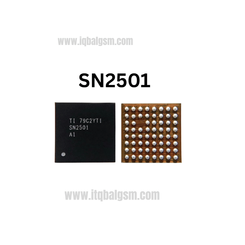
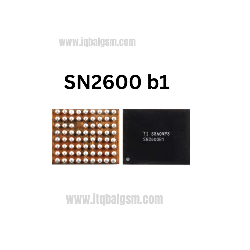
56030 IC
As low as
Rs 250.00
Worldwide shipping · Cash on Delivery
Product Details
--------------------------------------------------------------------------------
SECTION 1: ELECTRICAL TOPOLOGY & RF FRONT-END ARCHITECTURE
--------------------------------------------------------------------------------
1. Signal Paths:
- RF Input (TX_IN): Receives modulated, low-amplitude RF signals from the Transceiver (e.g., WTR2965, SDR660, or MediaTek MT6177/MT6186).
- RF Output (TX_OUT): Outputs high-power amplified RF bursts directly to multi-plexers, duplexer banks, and the antenna switch matrix (ASM).
- Control Interface (MIPI RFFE Bus): Dual-line serial interface (VIO 1.8V, SCLK, SDATA) managed by the Baseband processor to configure gain steps, power modes (High/Mid/Low), and band selection.
2. Power Rails:
- VBAT / VPA_APT: Main supply input from Average Power Tracking (APT) DC-DC buck converter. Supplies up to 3.4V - 4.5V DC with peak current spikes exceeding 1.8A during LTE transmission.
- VIO / VDD: Regulated 1.8V logic rail for internal bias and MIPI control registers.
--------------------------------------------------------------------------------
SECTION 2: BOARD-LEVEL DIAGNOSTICS & MULTIMETER MEASUREMENTS
--------------------------------------------------------------------------------
1. Cold Testing (Diode Mode Drop Readings - RED probe on GND, BLACK probe on test points):
- Main VPA / VBAT Power Capacitor (Large capacitor adjacent to QM56030):
* Normal Reading: ~360 mV to 480 mV (Resistance mode must read >1.5 kΩ).
* Defective Reading: A reading of 0.000V or under 30Ω indicates a shorted internal gallium arsenide (GaAs) / CMOS power transistor.
- 1.8V VIO Logic Filter Capacitor:
* Normal Reading: ~450 mV to 580 mV.
- RFFE Control Lines (CLK / DATA):
* Normal Reading: ~480 mV to 600 mV with balanced values on both lines.
- RF TX Input / Output DC-blocking Capacitors:
* Normal Reading: ~400 mV to 550 mV on active side; open/capacitive on RF side.
2. Hot Voltage Testing (Board Powered with SIM Card Inserted):
- Measure VPA Supply Rail: Steady +3.4V to +4.0V DC during standby.
- During outgoing call initiation: Observe DC current meter on power supply. Current should ramp up smoothly from ~180mA to ~450mA. If the phone draws >1.2A and instantly shuts down or drops to 0 bars, QM56030 is burned internally.
--------------------------------------------------------------------------------
SECTION 3: REWORK, DESOLDERING & INSTALLATION GUIDELINES
--------------------------------------------------------------------------------
1. Chip Removal:
- Apply heat-shielding Kapton tape and thick aluminum foil over neighboring components, especially the CPU, UFS/eMMC, and sensitive crystal oscillators.
- Apply high-grade tacky flux (Amtech NC-559 or Relife RL-422) around the perimeter of the QM56030 module.
- Hot Air Settings: Set temperature to 330°C - 340°C with 25% airflow.
- Heat in a smooth, continuous circular motion for 15–20 seconds (PA modules have a large ground thermal pad underneath that dissipates heat rapidly).
- Lift vertically using precision curved tweezers without scraping adjacent micro-resistors.
2. PCB Pad Preparation:
- Use a chisel soldering iron tip at 320°C with leaded solder wire (Sn63/Pb37) to remove the high-temperature lead-free factory solder.
- Clean the ground plane and perimeter signal pads with 0.8mm desoldering braid.
- Ensure the ground pad is completely flat to avoid the chip sitting tilted during installation.
- Clean thoroughly with 99.9% pure Isopropyl Alcohol (IPA) and inspect under microscope.
3. Reballing / New Chip Soldering:
- Use a dedicated universal PA stencil (0.12mm thickness) with 183°C medium-temperature solder paste if re-using an IC. New factory chips in blister tape come pre-tinned.
- Apply a micro-thin layer of flux on the PCB footprint.
- Align the Pin 1 orientation marker (dot/corner notch) accurately with the motherboard silkscreen white dot.
- Heat with hot air at 320°C with low airflow (15% - 20%) to avoid blowing the chip away.
- Watch for the solder to melt and verify self-alignment; gently nudge the corner with tweezers to confirm surface tension lock.
- Allow the motherboard to cool down naturally for 2–3 minutes, reconnect all coaxial antenna cables firmly, install the back cover with antenna springs, and verify full 4G LTE signal bars and successful outgoing voice calls without signal drop.
You may also like